PCBWay is a PCB manufacturer that prides itself on quick turnaround. You can learn about CNLohr’s sucess story here. They also offer detailed tracking of your order’s progress on their website.
They have reached out to me and kindly offered to sponsor the boards for this particular project, which I will be talking about in the coming weeks. As the cost of these boards were more expensive (compared to their “normal” orders), I had to pay for shipping myself.
With each PCB project, I find more and more methods of testing PCB manufacturers. This time, it’s with a PCB that is inserted directly into your USB socket.
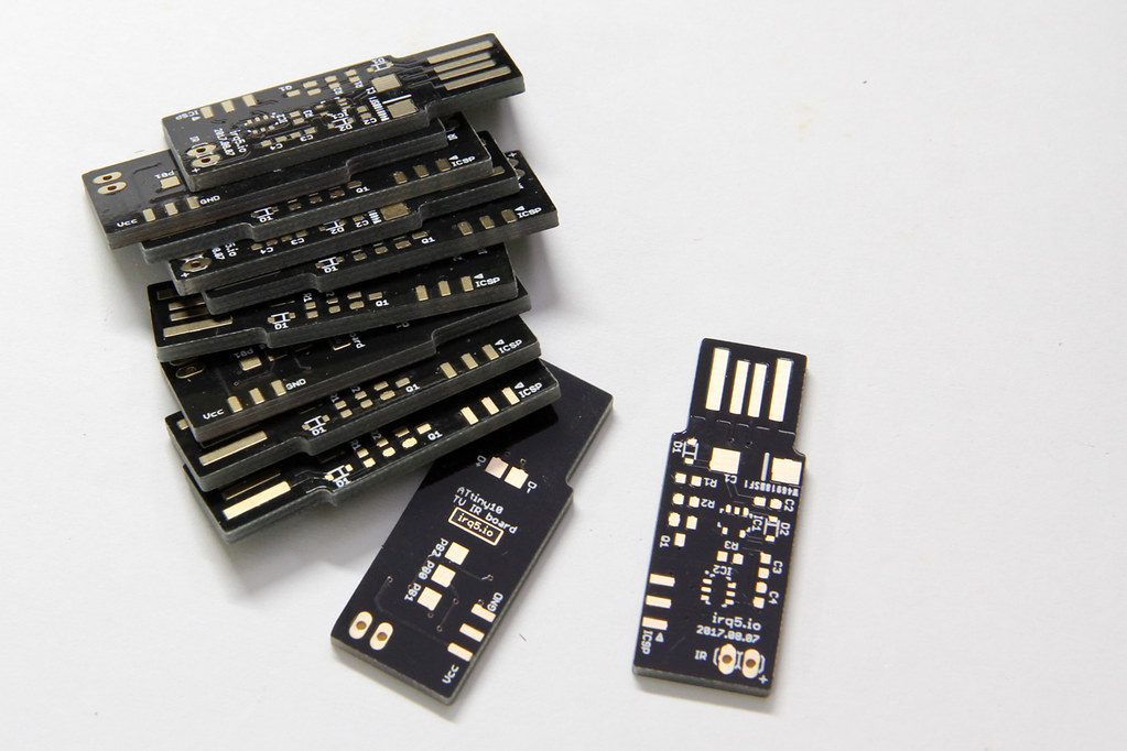
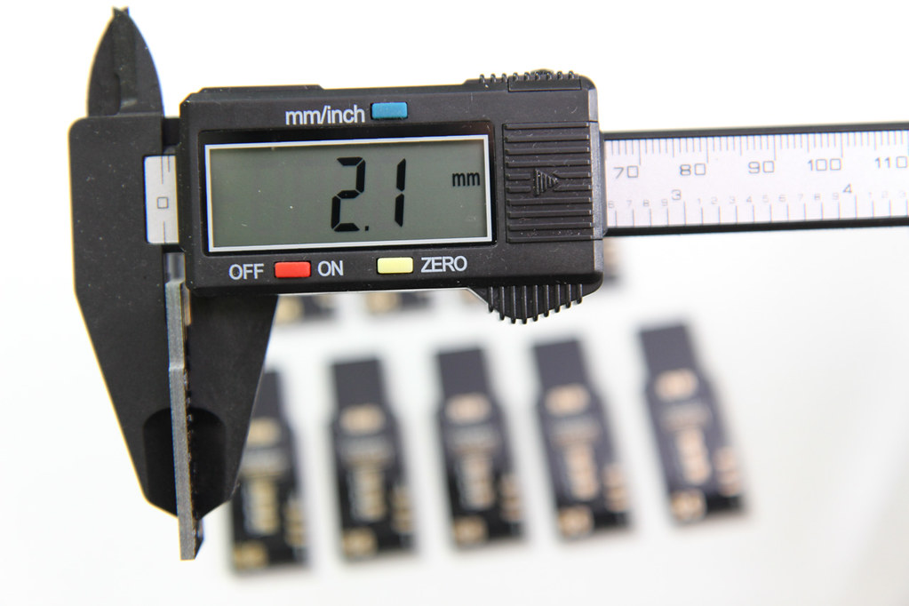
The requirement for such a board is 2 mm thickness. The USB connector size is standard, so the usual 1.6 mm PCB thickness isn’t going to work unless you pad the connector area.
Also, I opted for gold fingers on the USB connector contacts. This is usually done for contacts on the board edge that will be inserted into some mating connector (like PCI cards and USB connectors such as this).
They also offer matte black & matte green colors. I haven’t seen matte colours being offered at other board houses so far. I would have loved to try them out, but that would have bloated the cost beyond my comfort level.
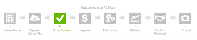
Order Process
The order flow for PCBWay is a bit different because you submit your gerbers without making payment first. This allows their engineers to take a look at the design before you actually pay.
Most other systems I’ve used are largely automated. After you submit your gerbers, they typically don’t expect any problems and so they collect payment from you first.
I uploaded the gerbers on the 8th Aug and I tracked my order progress online. Their website allows you to track the detailed progress of your board as it moves along the manufacturing process. For small runs like this one, it is not crucial but if you were doing a large project with panels of many boards, this would definitely be handy.
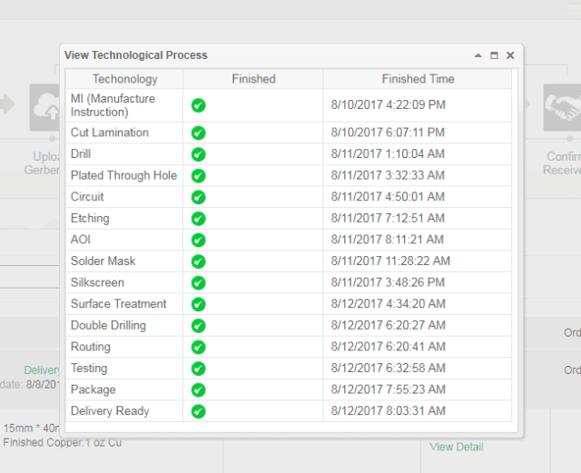
They started manufacture 2 days later (on the 10th) and completed everything by 12th. It was not until the 14th that they actually shipped the boards out and provided me with a tracking number.
Here’s a summary of the timeline:
- 08: Gerber files submission
- 10: start of PCB manufacture
- 12: boards completed
- 14: boards shipped (via registered post)
- 24: boards received
Cost
The price for “standard” PCBs are $5, 10 × 10 cm 2-layer boards. This is a pretty typical (low) price these days for such prototype PCBs.
Where possible, you should design for 6mil minimum track spacing and 0.3 mm minimum hole size to avoid extra costs. This is true for both PCBWay and Seeedstudio that I tested previously. DRC rules can assist to ensure these design rules constraints are met, so you don’t get charged extra, and/or the board house doesn’t encounter problems during manufacture.
When I opted for an ENIG surface finish, the price went up to $38 (+ $33).
Because we need the board thickness to be 2 mm instead of the usual 1.6 mm, it further increased the price to $69 (+ $31).
Shipping
I opted for the registered mail, so that adds another $10 for the shipping fee. This is slower than delivery services like FedEx/DHL, but less costly since we are not in a hurry.
The PCBWay box is wrapped in a copious amount of tape (typical for most China parcels) sent via registered post, which usually takes a few weeks to arrive. In my case, the order was shipped out on the 14th and arrived 10 days later on the 24th, still pretty fast but your mileage may vary.

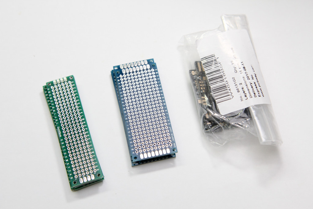
It came with some free prototyping boards, as well as our ordered boards. The PCBs were all just loose in a plastic bag there, no padding material, shrink or bubble wrap. It’s not exactly a big problem because the PCBs are pretty hardy.
Findings
The produced boards are generally OK:
- Drilled holes & vias are good, means they made it properly to their own specified minimum clearances
-
Solder mask has not been intentionally reduced. Some board houses might do that, resulting in no solder mask between the pads of small pin pitch components like a SOT-23
-
No misaligned or badly offset silkscreen, like the ones I’ve seen previously on Seeedstudio boards.
However, there are some other points that are worth mentioning.
Board Thickness
The board thickness was on-point, 2 to 2.1 mm. I have also tested it by sticking the board into various USB sockets, on my PC, on the Pi, etc. Anyway, the measurement with plastic calipers should always be taken with a pinch of salt.
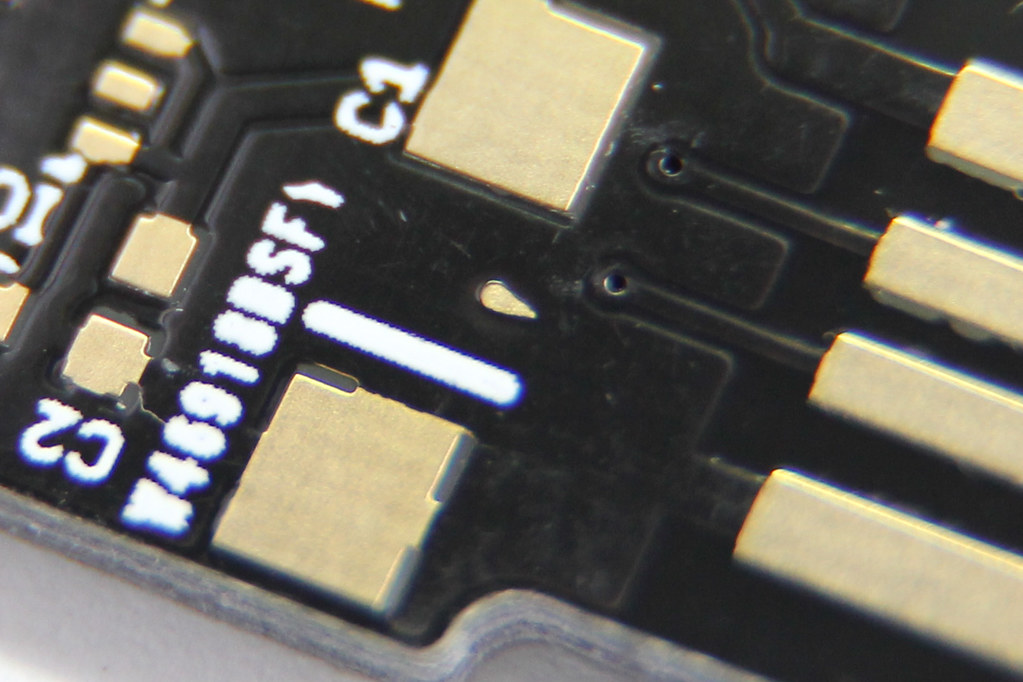
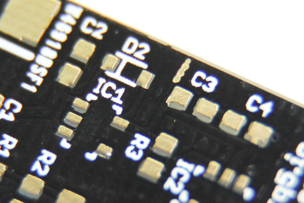
Random Exposed Copper
Not sure what was happening here but the boards had random bits of odd-shaped exposed copper areas on some boards.
On one board, there is a teardrop-shaped exposed copper between the two large pads of C1. On another board, it’s a ribbed line beside the C3 component marking.
Fortunately, these exposed copper areas are not under a component that might cause a short. Otherwise, that board would be unusable.
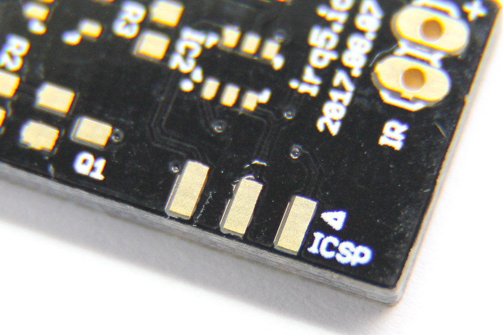
Solder Mask Weirdness
The outline of the black solder mask is jagged around some pads, but perfectly clean and straight on others. In other boards that I have manufactured, the solder mask around pads and holes has clean, crisp edges.
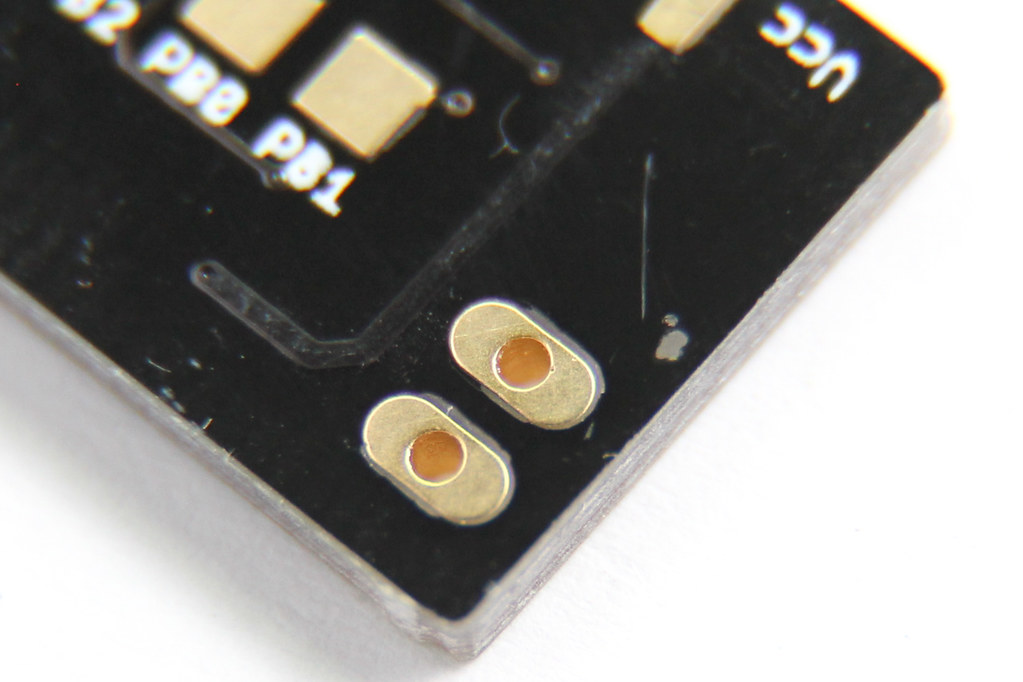
In the close-up below, you can see a sliver of the exposed ground plane around the edges of the ICSP pads.
This problem can also be seen on another board, around the D+/D- pads as well as the website “logo art”.
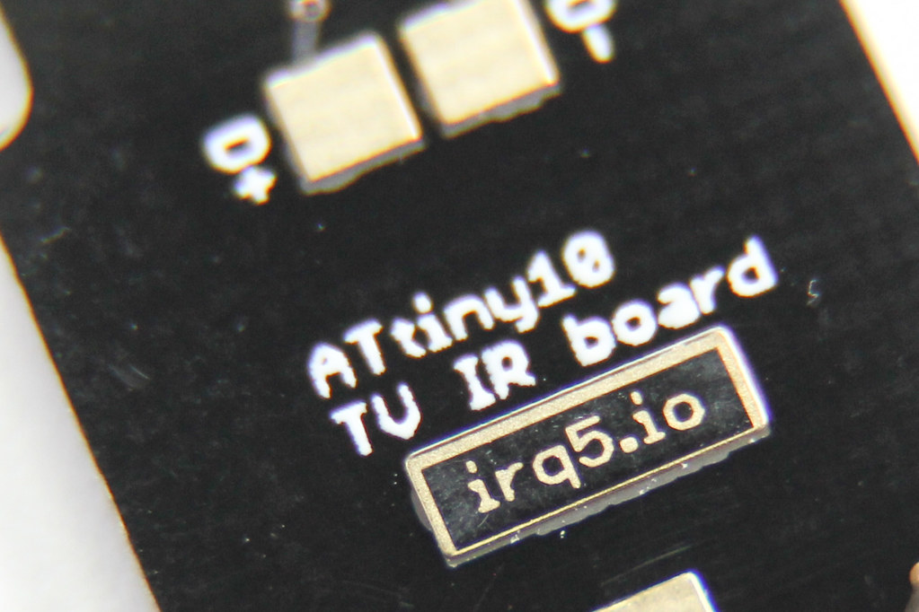
On another board, there’s even a hole in the black solder mask. Also, note that the solder mask cutout for the oval pads are not clean.
As long as it does not exposed copper that was not supposed to be exposed, it shouldn’t pose a problem. In the case of these boards, it is fortunate that the random copper bits do not short out any components.
Gold Fingers?
I saw this option indicated on the order form, so of course I opted “yes” because I know this board acts as USB connector and I want it to be durable.
Essentially “gold fingers” is a hard gold plating for PCB edge connectors, so that these contacts on the board edge can withstand a greater number of repeated insertion cycles. This is typically done for expansion cards that are forcefully inserted into a connector, like PCI cards and of course, USB connectors. The best, most detailed description I’ve seen so far is by Eurocircuits.
Looking at the received boards, there is no visual indication that the edge contacts were electroplated. For electroplating, you need to pass electricity through the contact, which is why sometimes edge connectors have traces that go off the board edgde. Also, I was not asked which region(s) was considered to be the “fingers” (this board was designed with two edge connectors: the USB and the ICSP connector). To plate everything with thicker gold is expensive, so it is definitely in the best interest of PCB houses to ask you for these regions to plate, rather than guess.
Based on these reasons, I doubt that the USB contacts were actually given the “gold fingers” treatment, although without a thorough analysis, it would be impossible for me to conclude that such treatment was or was not performed. They could have increased the gold plating thickness during the ENIG process, but going back to the problem of additional cost (to them), it seems rather unlikely.
Conclusion
Well, aside from the highlighted problems with these boards, PCBWay generally makes decent PCBs. Their prototype PCBs for hobbyists (like myself) is competitively priced at $5.
If you are looking to manufacture PCBs with a matte black or matte green solder mask, or if you need a fast turnaround time like CNLohr, I would recommend you to give PCBWay a try.
You can also find more PCB photos in my Flickr album.
Also, stay tuned for the write-up of this project in the coming weeks!

bad company take your money do not deal with them
Order ID: G362815 Delivery Address
Order time & date : 2019/1/27 17:57:38
Sorry this is not a support forum or a place for complaints. Nobody knows the circumstances or details surrounding your order, so your comment is not helpful to my readers; it will be removed soon. If you have any problem with your PCBway orders, please contact them directly.