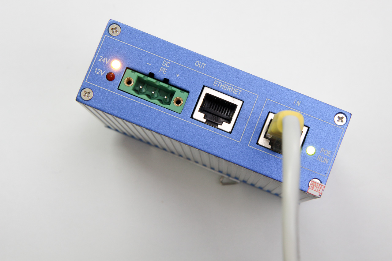
Continuing my PoE series, I bought the ONV PD3401G, an active PoE splitter that is capable of extracting up to 60W (24V @ 2.5A) from the PSE. It is housed in a small aluminum extruded case that can be DIN rail mounted. This splitter is comparatively low-cost, about US$35, and more importantly, is capable of passing through Gigabit.
ONV seems to be quite a reputable company, so I believe their products shouldn’t be too badly designed. This unit can also be easily purchased on Aliexpress without having to go through some obscure distributor.

Internally it uses the LT4275A (marking LTGBT) for PD interfacing. The A variant of this chip supports up to 90W of power. On the power supply side, it uses a NCP1034 synchronous buck converter. The NCP1034 is capable of handling up to 100V, which is more than sufficient for PoE.
Looking inside, the in/out Ethernet ports are connected via a transformer, in order extract power from the center taps of each pair. We can see that the PCB traces for the input port pairs are thicker to carry the higher currents. Large beefy diodes form rectifier bridges for the data pairs.

Surrounding the input port on the underside, there are a lot of unpopulated components; those were supposed to offer input protection, probably using some TVS of some kind. these are marked RD1 ~ RD8, one for each Ethernet wire.
The “POE RUN” LED which indicates PoE power input, is powered by the incoming 48-57V PoE voltage running through a high power resistor. It’s not really ideal, but i think this might also help with loading on the PD side to cope with the minimum power draw.
The 24V/12V LED indicator is also hard-wired, rather than using some fancy comparator circuitry which increases cost. Someone at the factory had to hand-solder either the front panel LED indicator and/or the correct resistor because there’s some flux residue in that area on an otherwise clean board.
The front panel LEDs are also overly bright. If you wish to place this unit somewhere in your living space, you might want to consider covering the LEDs with duct tape or something.

You can see more photos on the Flickr album here.
PD Interfacing
The designers helpfully included a handy table of resistor values (R7 & R8) for different PD identification signatures. In this case, it identifies as a 90W LTPoE++1 PD.

The signature output pin (T2P) should have been used to interface with the output regulator for current limiting, in the case where the PSE can only supply lower currents like 13W or 25.5W. This implementation just assumes that the PSE will always be able to provide the high current, or none at all. Drawing too much current will likely cause the PSE to cut power, killing the entire unit and having to restart the PD negotiation again. Sure this works, but It’s just not a good design (if there was any “design” at all).
The unused open-drain outputs are just being pulled-up to Vcc with a 100K resistor.
Power Supply Section
There are various places on the board where the solder mask have been stripped. These allow for solder to be added to the traces to increase current carrying capacity.

The NCP1034 uses two N-channel MOSFETs, so in this design both have been chosen to be the same — 60N10 — one of those “jellybean parts”, it seems. The large PCB pads for heat dissipation are not really used. Instead, the high-side MOSFET is just free-standing (“flapping around in the breeze”), and the low-side MOSFET has its own free-standing heatsink. As the case is fully enclosed, there is no airflow within the case, so the heat won’t be efficiently dissipated. They should have designed the MOSFETs to be thermally coupled onto the case for better heat dissipation. According to ONV’s product datasheet, it quotes an MTBF of 190,000 hours (about 21 years).
The output voltage of the regulator is controlled by resistor divider R15 & R16, located on the back side of the board. This model uses 182K and 10K, which gives exactly 24V, when coupled with the internal reference of 1.25V. There is also a 12V output variant of this PoE splitter, which presumably uses different resistor values for the divider.
The NCP1034 has a SS/SD (soft start / shutdown) pin, but that’s just tied to a capacitor to provide for soft-start. The NCP1034 does have a few UVLO circuits that prevent the MOSFETs from operating outside some predetermined conditions, so they are just relying on that.
Everything else is pretty textbook.
Output Voltage Mod
As I have mentioned in my PoE Quick Guide, trying to get PoE splitters in non-standard output voltages is quite difficult (and that translates to being expensive).
Since this splitter is based on the NCP1034, we can adjust the output voltage ourselves with help from the datasheet.
The output voltage is given by Vref * (1 + R1/R2), so if you use the current resistor values R1=182K and R2=10K, we get 24V exactly, less tolerances. To change the output voltage, we need to adjust the values of these resistors accordingly. However, this resistive divider ties in with the compensation circuit.
The compensation circuit used here is of the “Type III (PID)” kind. Their values are dependent on R15 (R1 in the datasheet) because they are placed in parallel. If you wish to alter the output voltage, it is therefore recommended to change only R16 (referred to as R2) because compensation only depends on R1. Due to these constraints, you might not get the accurate output voltage you want, but at least you won’t have to re-calculate the compensation network values.
I attempted to work out the values to make sure the compensation equations were still valid, but either the values I measured in-situ were wrong, or the values didn’t really conform to the equations in the first place. Here they are anyway, for your convenience:
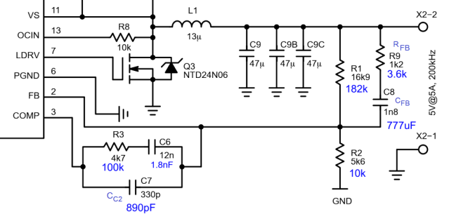
Anyway, if we wanted a 18V output, we calculate for a new R2 value like so:
R2 = Vref / (Vout - Vref) * R1
   = 13.582...
The closest valued resistor I could buy is either a 13.3 or 13.7K; with these, you either get ~17.85V or ~18.35V. To get closer to 18V, I decided to get use 13.5K, which could be achieved by stacking two 27K resistors in parallel, yielding an output of ~18.102V.

Using a small DC load tester, the output voltage seems to be maintained when approaching a 2W current draw, although I don’t know about the ripple.
I don’t have any proper equipment to test higher currents for a sustained period, but I will report back if there are any developments on this unit.
Verdict
The splitter caused no problems with the Gigabit speed, so I assume it’s properly designed — the traces are of matched length, and the transformer parameters were correctly chosen.
The unit is compact, relatively low-cost and works as expected. As an added bonus, you now have the means to modify the output voltage of this splitter easily.
Overall the implementation is passable, with a few things that could be improved. Here are some drawbacks I found from evaluating the design:
- Blindingly bright LED indicators. I am clearly not the only one who has an issue with this, @marcan42 recently talked about the appropriate brightness levels for LED indicators as well.
-
Non-isolated supply. Technically PoE splitters should use an isolated DC-DC regulator, since the Ethernet data signals themselves are already isolated. However, if you are connecting to wireless equipment or other equipment that will not connect to more devices physically (electrically), then that should be fine.
-
Possible over-current of PSE supply. Because the power supply section is functionally isolated from the PD controller, it may try to supply more current to the downstream device than the PSE can provide. There should already be current-limiting on the PSE supply, which shouldn’t be a big problem but still, this non-compliant PD behaviour can and should be fixed.
-
Shorter-than-ideal lifespan. Heat always shortens the lifespan of electronics. This device could theoretically last much longer if the MOSFETs had their bodies somehow affixed to the exterior aluminium case for heatsinking. Having the MOSFETs just free-standing inside a closed aluminium case with no airflow just doesn’t help to cool it.
If you did find this review useful or have any questions, please feel free to leave a comment below.
- 802.3bt was not yet standardized when this chip came out, so they came up with LTPoE++ as their stop-gap implementation ↩

Thank you very much for your thourough investigation!
I applied your formula and made a 24V splitter out of a 12V. The formula proved correct. I had a original 24V but I had damaged it, so it was a quick solution. What I can share with you is that in the 24V the R and C Values are diffrent, they adopted R16 and 16 and the network as you descibed. Important is that I had tou change R14 to 7k5, I moved it from the original 24V version to the modified 12V. Without, it faied to start up under load (2x21W 12V in series).
after about 8 hours under 50W load it stille works fine. Thanks for your input and maybe R14 needs a bit extra attention in your article.
E, The Netherlands
Thanks for sharing the information you have on the 12V version! I believe R14 is tied to the OCset pin, which limits the output current. I’m glad I was somehow able to help you with your unit.
Extra info about he values:
R14 = in 24V version: 7501 (18.2k); at 12V version: 4701 (4k7). To modify 12V original to 24V use 7501.
R15 = in 24V version: 1823 (18.2k); at 12V version: 4422 (44.2k, measured on PCB about 33k). Left unchanged as advised.
R16 = in 24V version: 1002 (10k); at 12 V version: 5111(5.11k). To modify 12V original to 24V use 2331.
R17 = in 24V version: 3601 (3k6); at 12V version 1211 (1k21). Left unchanged.
Do you have a link to the datasheet where you found the reference scheme?
E, The Netherlands
BTW: Any suggestions how I could repair the 24V, I shortened it a couple of times, would the jellybean Q3B then Q2B, then Q1A be the first victims to test/replace?
I would think to try replacing the output driver MOSFETs as you suggested. Do let me know if you are successful!
Correction, I wrote for R16 (6 Jun 2019 at 3:45 pm) ” To modify 12V original to 24V use 2331.”
That was a typo. R16 must be 2431 (2.43kΩ, E96 series). I used 2x10k+2x220ohm metalfilm and selected them to be around 2435 wich gives me 24.0-24.2 Volt output.
I already found the datasheet at https://www.onsemi.com/pub/Collateral/NCP1034-D.PDF 🙂
Thanks again for putting me on the right track!