I had these chips extracted from the old motherboards I threw away some time ago, and I thought I’d have some use for them some day.

These are Electrically Erasable and Programmable Read-Only Memory (EEPROM) chips which are used to hold the BIOS code. I was curious to find out what’s in these chips and if I could re-use them for storage in my projects, so I decided to interface with them.
Basically these EEPROMs follow a standard pinout for a given capacity. These EEPROMs I have are 256KByte (256K x 8 as described in the datasheet), and one of them is 128KB. The pinout can be found in the datasheet – I’ll just mention one part number here: Winbond W49F002U. These chips expose an interface pretty much like standard SRAMs (which was covered in my course), with a 8-bit data bus and 18-bit (or 17-bit for 128K) address bus interface, along with WE, CE (alternatively known as CS), and OE.
As you can see from the pictures, there’s a lot of pins to hook up. Usually only microcontrollers with a higher pin count which has some virtual memory space will allow easy interaction with such chips. I could also hook up this chip to something like an ISA bus on a PC and write some code maybe in DOS to interface with the chips directly. However I only have an Arduino lying around.
These chips have 32 pins, if you leave out the supply pins there’s still 30. The Arduino doesn’t have that many pins. I’ve seen circuits around for EEPROM readers or progammers. These can be categorized into 2 groups – one using a counter for the address bus, and the other using shift registers. The one that employs a counter uses a ‘4040 chip, which is a 12-bit binary counter. With 2 of these, they could generate up to 24-bits – more than what we need. The other variant uses an 8-bit shift register, which gives us 16-bits if we use two.
I decided to use a shift register, as these EEPROM chips support magic codes on the address bus for some special functions like sector protection, chip erase, etc. The codes are specifically 0x5555 and 0x2AAA, which if a counter was used, needed 20,000+ or 10,000+ clock pulses respectively. If a shift register was used, we need only a constant amount of pulses for any address, which is 16 to shift all the 16-bits. In normal read/write cycles, the address is simply incremented or decremented with every read/write – very rarely do we need to set arbitrary addresses. The drawback for this approach is that we spend extra cycles during normal read/write sequences – instead of a single pulse to increase the counter, we need to set all 16-bits of the address.
With so many pins, I decided to try getting an SOIC version of the shift register since it would definitely be cheaper too. There’s a few shift registers to choose from – 74HC164 or the 74HC595. The ‘164 costs $0.80 to $1, and the 595 costs $0.25. Of course I just went ahead to pick the cheaper part but this is not without its drawbacks.
The ‘164 output changes as soon as the bits are shifted in, but the ‘595 has an additional latch in front of the bits. The ‘595 has an additional clock-like input which controls the latch behaviour. A positive going transition is needed to cause the latch to be updated with the newly-shifted bits. This is more flexible but also means it has more pins to interface with because I cannot just tie this pin high. The ‘595 is also very suited for an address bus chip because it allows the outputs to be tri-stated, but of course it doesn’t matter for this project.
This is my first time working with SOIC components – I usually use through-hole 0.1″ components. Using a veroboard (or prototyping board or whatever you call it), you need to cut the pads into half so they do not have any electrical connection. This can be done using a pen-knife or XACTO knife. Use a multimeter to verify this after you’re done.

The IC fits really nicely across 3 rows of pads. You will notice half of the pad is under the IC. You have to make very very sure that the pads are not connected, especially underneath the IC. After soldering all 16 pins, I realised that one set of adjacent pins was short-circuited, and the problem was isolated to under the IC, which I could not access. I had no choice but to lift one of the pins off the pad. Very very bad. As you solder the pins, continually check for short-circuits that may form. Fortunately the ICs were not damaged.

This is the completed wiring, along with a 5-cent coin (if you know where this is from) for comparison. It was really tedious wiring up the whole thing. White wires are the data bus D0~7, the gray wires are the lower bits of the address bus (A0~7) and the yellow wires are the upper bits (A8~15).
The row at the top are header pins (which you will see later) which connects to the microcontroller, and below that are the 2 shift registers for the 16-bit address bus, and in the lower section is the 32-pin DIP socket for the EEPROM.
I used an Arduino to hook up to this interface board. I find the ribbon cable really handy, which I made out of old PATA interface cables. The EEPROM interface board has the 8-bit data bus at the furthest edge, followed by the EEPROM control pins like WE, CE and OE which I tied directly to Vcc or GND as required for reading, and 4 pins to control the shift registers (reset, data, clock, latch clock), as well as power from the Arduino board.

The schematic of the board looks like this:
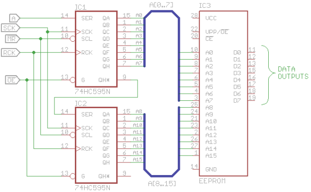
On the left, Arduino output pins drive the cascaded shift registers IC1 and IC2 for the address bus, while on the right, the EEPROM’s data output pins are connected back to the Arduino to be read.
Looking at the Arduino pin mapping, I couldn’t find a port with all 8-bits exposed, so I broke up the data “bus” into two lower halves of PORTB and PORTC. This is because it’s much faster to access the ports directly using PORTx rather than to use the digitalWrite & digitalRead functions. It’s funny how I use an Arduino but I write code like I’m programming an ATmega168 directly.
You’ll notice a blue wire that was inserted directly into the EEPROM socket. This is because the address bus only generates up to 16-bits but the EEPROM has up to 18-bits. This EEPROM is 128K only, so it has a 17-bit address bus. The 17-th bit (A16) is being controlled by that blue wire.
The Arduino starts bit-shifting the bits into the shift register and reads the data from PORTB and PORTC and spews it out to the serial console. After each read, the address is incremented and the cycle continues until all the data has been read. I then swap the blue wire from GND to Vcc, and repeat the read cycle to read the upper 64K.
Looking at the amount of work required to wire up the EEPROM, I’m better off using a serial EEPROM for storage instead. However such a chip is still handy for making things like this DDS waveform generator.

I was very interested. Any diagram for me to try to ride one of these?
Hi, thank you for sharing your experience. I have one Winbond W49F002U-12B. And I would like to use it somehow :D. Could you please share the source code for your arduino?
Hi, sorry I couldn’t find the Arduino code for this reader – it has been a while since I have used it. But the theory of operation is simple: it shifts in an address starting from 0 and the EEPROM data output will contain the byte at that address location, which is then read and sent over the serial port. The Arduino sketch then increments the address and repeats the process for the next byte (and so on). I had a simple program running on the PC to that reads these bytes from the serial port and writes them to a file. Unfortunately I can’t find the Arduino sketch nor PC program.