Fusion PCB is a PCB service from Seeedstudio. They have been offering PCB prototyping service since I made my first board in 2011. It has recently been revamped a little, tweaking prices and options, as well as integrating an online Gerber viewer from EasyEDA. I was invited to give Seeedstudio’s revamped Fusion PCB service a try, and since I had some boards in the pipeline for manufacture, I thought why not?
You can configure various options for the PCB, such as board thickness, copper pour and surface finish. You can also make flex PCBs or aluminium for better heat sinking, as opposed to regular FR4. These options will of course come at a price. However, you can select various colours for your PCB at no additional cost.
The Boards
I ordered 2 sets of boards in total. I’ve decided to opt for an ENIG finish for the TIL311 display boards, just because it looks nicer in gold. The boards are manufactured with black solder mask, making the gold pads stand out better.
I’ll describe the display board in a separate post after I’ve assembled it. For now, here’s what 4 of the boards look like, component side up:
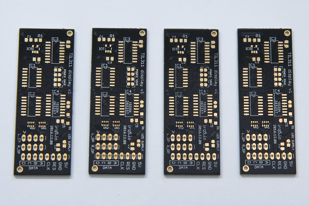
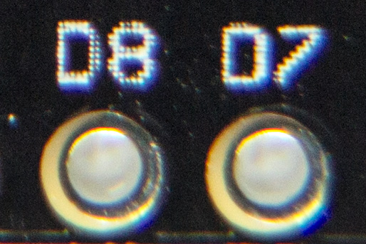
Like most PCB prototyping services, they track your order by printing some kind of order identifier onto each PCB. Usually they try to put this identifier underneath a component like an IC so it gets hidden when the board is fully populated, but sometimes they put it somewhere prominent, like under your product name. On this board, the identifier sits under IC4 but for the other board, it was under the product name.
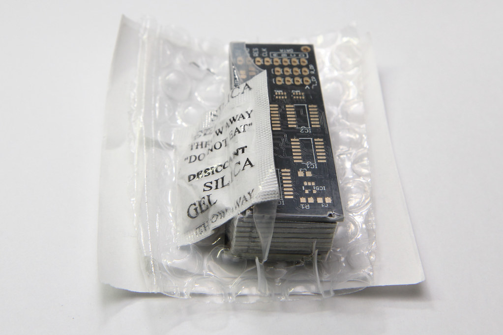
The PCBs arrived in a shrink-wrapped bubbly packaging to protect the boards. There was also a desiccant thrown in for one set of the boards to keep it dry.
Layer Alignment
Since PCBs are composed of several layers, built up using different processes, it is important that these layers all line up accurately. There is the copper layer, the solder mask layer, followed by the silkscreen layer and of course, the holes for vias and through-hole components.
For some reason, 9 out of the set of 10 boards for this TIL311 display had badly offset silkscreen; only one of the boards had correctly-positioned silkscreen. Since the silkscreen is the last layer to be applied, you can see they’ve printed it onto the copper as well.
The silkscreen alignment issue is evident in the photo above, as well as a close-up of the header area:
Here’s what it should have looked like. This is the only one board (out of 10) that had the silkscreen correctly positioned.
In 3 batches of our XCTF badge runs from DirtyPCBs, we have not seen any kind of silkscreen mis-alignment this bad. I must have been really lucky to encounter such a run.
The solder mask was also offset on one of the boards, revealing parts of the ground plane copper that was not supposed to be exposed. Here’s a close-up of the PCB, as well as a 3D rendering for comparison:
Tight Tolerances
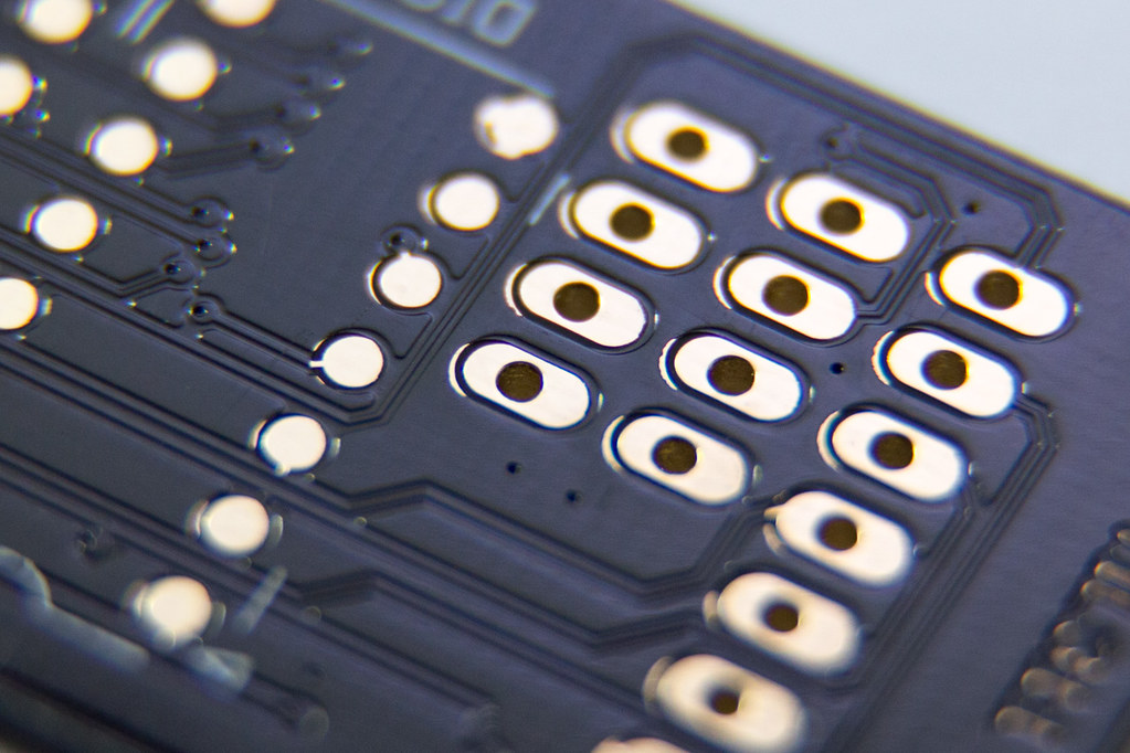
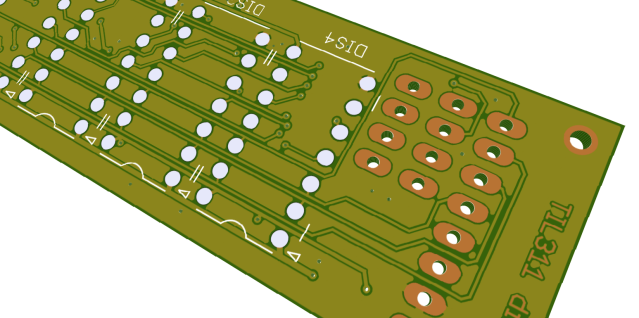
This has to be one of the tightest board layout I have tried my hand at making. (Maybe that’s because I’ve only made simple breakout boards so far.) In this display board, I’ve had to resort to using 0.16mm (6.3 thou/mil) traces and snaking them between SOIC pins and 0.1 inch spaced pins because I wanted to keep only the displays on the front and the remaining components on the back side. The traces should meet Fusion PCB’s specified capability of 6/6 mil. The holes for the vias are also testing their limits, at 0.3mm. You can see it in the close-up and rendering above.
On a cursory visual inspection, these traces seem to be fine — no shorts and there is solder mask over traces that run between the SOIC pads (very important). The site makes no mention of electrical testing (E-Test), but if there was E-Testing done, opens and shorts between electrical nets would have been checked for using an automated process.
One slight nit is that only on their order page (where you upload the gerbers) do they actually specify the minimum tracking/spacing of 6/6 mil. Their FAQ (in various places) on PCB specifications incorrectly states 4/4 mil, which would cause an additional fee to be imposed on your order for these tighter requirements.
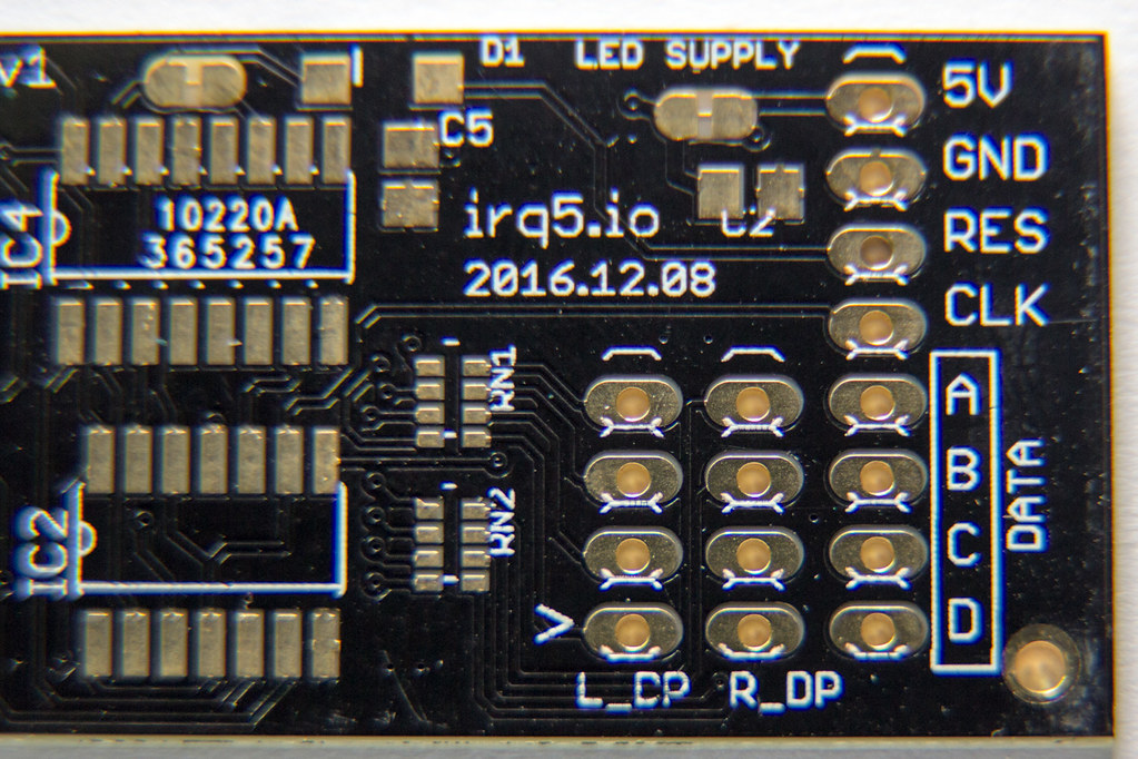
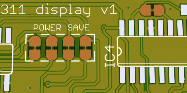
It’s interesting to note that they did put that little bit of solder mask over the thin bridge of the “power save” solder jumpers (correctly), as specified in the Gerber. But this is not very consistent because there isn’t any solder mask for that jumper above IC4. Here’s a close-up, as well as a rendering for comparison:
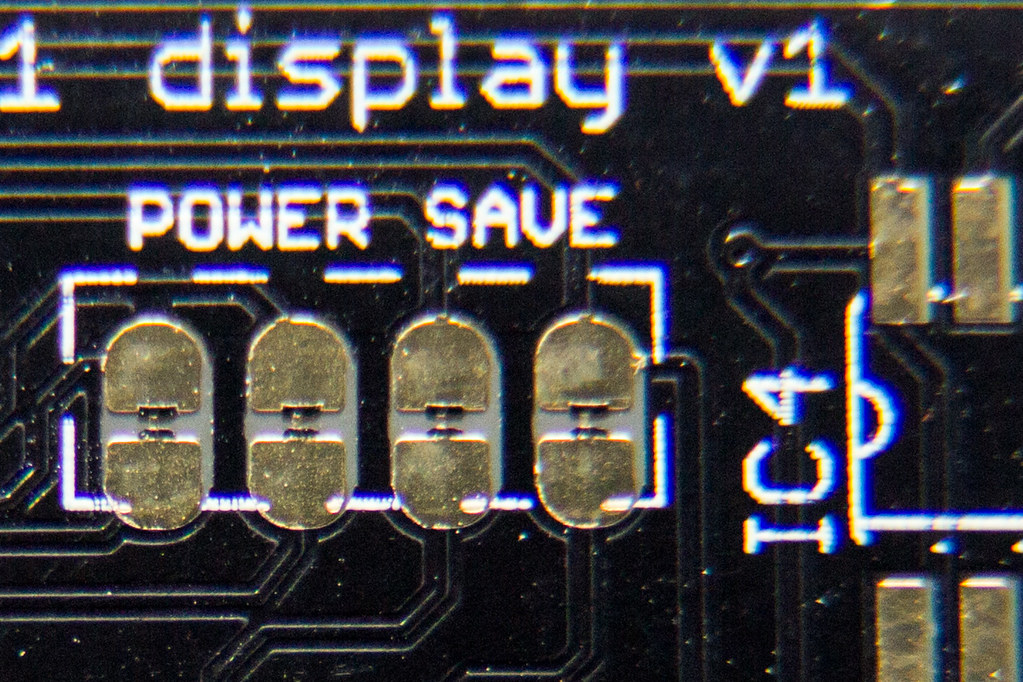
Once again in this close-up, you can see the silkscreen is offset and printed onto the copper pads of the solder jumper.
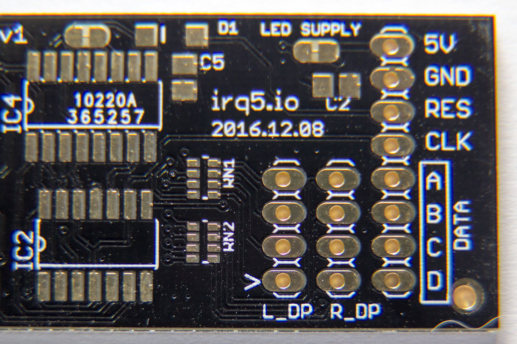
The silkscreen is printed using some inkjet technology, because for some boards the silkscreen was spotty (like it was running out of ink), so you can actually see that they print using dots. In the same picture, you can also see that the solder mask alignment is slightly off, but still OK — this occasionally happens with other board houses too.
Timeline
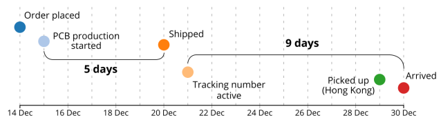
I placed the order on 14th December, and the boards arrived at my door on the 30th Dec. In total it took slightly longer than 2 weeks for an order to be delivered, but the actual time is going to vary between orders.
The PCB production took 5 days, as they have promised, but the shipping took a little longer than expected; I’ll explain why in the following section.
Shipping Options
I have ordered from Seeedstudio before, and my items were shipped with box type B00. Shipping only cost US$3+ for regular registered mail, although it did take a longer time to arrive — typical China postal service takes about 3 weeks to a month or so.
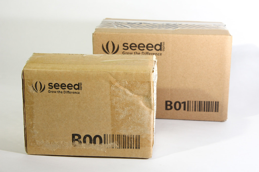
However, this time around, the shipping options was upwards of US$17. The PCBs came in a type B01 box, which is slightly larger, but I believe everything could have fitted into a B00. Perhaps shipping two sets of boards made it exceed the lowest weight bracket, but not that it would matter. For my order, FedEx and regular mail differed by $1, so obviously I went with FedEx because it was faster.
Shipping via FedEx would take 4-5 working days, whereas regular air mail would take 10 days or more. This timeline depicts the actual time taken for various parts of the order:
As you can see from the timeline, after the PCBs were shipped on the 20th, the FedEx tracking had no recorded activity, right up until the day before delivery. On the 29th, the package was picked up in Hong Kong, stopped over in Guangzhou in the early morning, and delivered the very next day before noon. So what happened to the package in the 9 days after it left the board house?
I think I figured it out. You can see it on the FedEx envelope as well:
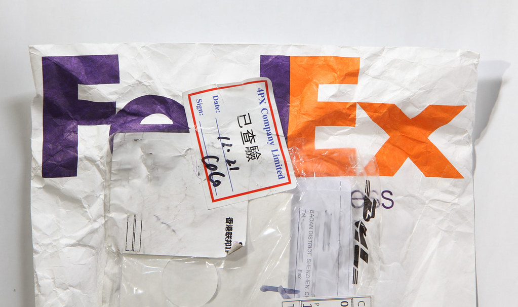
There was an inspection sticker from 4PX, which is a shipping company I’ve come to know because of the numerous stuff I’ve ordered from AliExpress. They received the package on or before the 21st Dec. During the time unaccounted for, the package must have been traveling from Shenzhen to Hong Kong, where FedEx picked it up for next-day delivery. This leg of the delivery was most likely not handled by FedEx because there was no tracking or updates recorded during this time.
The package was shipped using FedEx International Priority, which from their website says “1 to 3 business days” (although the Seeedstudio quotes 4-5 working days). You can see that FedEx does actually provide next-day delivery in our case, from pick up to package delivery. It is unfortunate that FedEx was not used end-to-end, but instead there is a middle man, which added to both the shipping cost and time.
Photos
Higher resolution photos of the PCBs are available for viewing in my Flickr album.
Conclusion
This review might sound harsher than my iteadstudio one, but I guess that’s because it was my first time making PCBs, the board was relatively simple and I didn’t know what to expect then. Now after several years passed and gaining some experience in doing this first hand, I have learned what to look out for. You should also note it’s not an apples-to-apples comparison because I’m not manufacturing the exact same PCB with both services in the same timeframe.
I’m not quite sure what to make of this Fusion PCB service. As you can see, my first order with them didn’t exactly give the best results. Shipping options were rather limited and more expensive when compared to similar services.
Nevertheless, Fusion PCB service does the job when you need to prototype PCBs. Their boards are decent, each one properly routed with no jagged edges, and seem to meet the tight requirements in terms of tracking/spacing, as well as drill holes. My other set of boards has rounded edges, and they routed the edges cleanly too.
Their pricing of the PCBs might be slightly lower compared to others, but the more expensive shipping erases this advantage. In order to be competitive with similar services, Seeedstudio should offer regular air mail priced similar to they used to offer, or what their competitors offer.
The next time when you’re making prototype PCBs, you can remember to include Fusion PCB as one of your choices. On top of the normal PCB prototyping, they also offer PCB Assembly (PCBA) service, which could be useful when you start manufacturing your product.
I have another set of boards to manufacture, so I might give DirtyPCBs a try next. I should get a better comparison of both PCB services after that, and I’ll report back. Stay tuned.

Doh! I read this 1 day after I sent my board to Seeed. *fingers crossed*
Should be fine. Let me know your thoughts after you get the boards!